8-bit Development Board for PIC18F45K50 MCU
My first introduction to the world of Embedded Software Development was through the extremely popular PIC12F675 – versatile, cheap, and most importantly readily available MCU in every electronics store here in Serbia. I’ve used it for more hobbyist-grade projects than I can count, and even managed to find a way to incorporate it into a low-power broadband RF Jammer, designed as a countermeasure for an “occult” eavesdropping method that involves capturing RF emanations from a monitor and reconstructing the image - usually from 10-20 meters away.
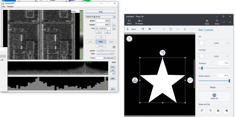
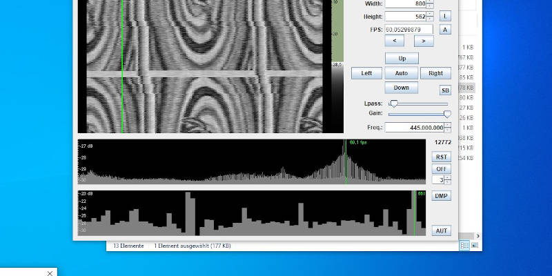
Below are the results of my trivial attempt at capturing and reconstructing RF emanations of a TFT monitor from two meters away. The attempt was an extremely low effort one - I used an RTL-SDR dongle and a random piece of wire as an antenna. While the quality is extremely poor, the drawn symbol is visible in the left image, and the default Kali Linux wallpaper is visible in the right one – albeit split. How much would the quality of the feed improve with a properly tuned antenna and an amplifier?
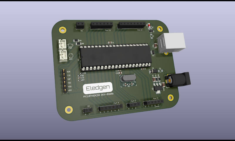
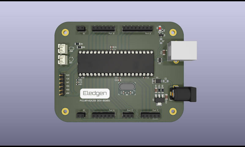
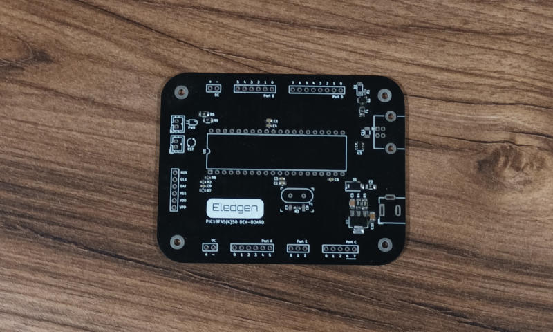
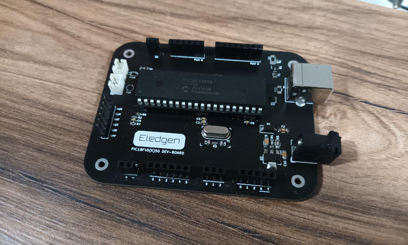
Having gained significant experience with programming and debugging 8-bit PIC microcontrollers, I decided to create a small batch of dev-boards based around the PIC18F45K50 MCU, which could be used as a foundation for prototyping anything that I may come up with in the future. Initially I wanted to over-engineer the board by adding a charger for Li-Po batteries, a 5V boost converter, length-match all of the GPIO pins - like it would make any significant difference, and even incorporate a 433 MHz RF TX/RX section. Ultimately, I chose to keep it simple.
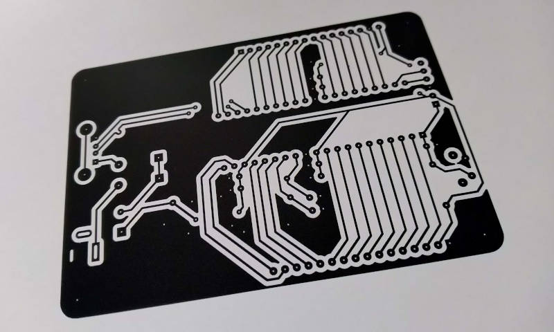
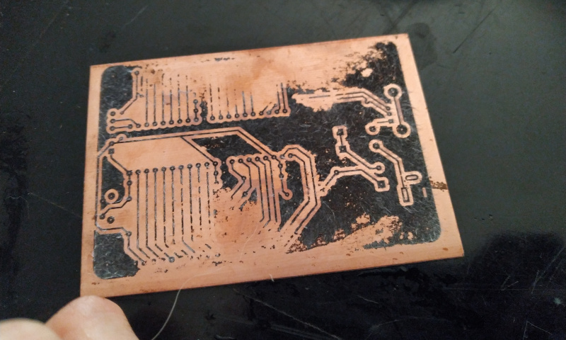
As usual, a prototype of the board was made using the toner transfer method and the, now obsolete, PIC18F4550 MCU that I had laying around - notice that the “K” is missing.
Horrible work, but necessary for gaining expertise needed for the more advanced projects I am doing these days - call it a stepping stone. MCU, Crystal & DC Jack were scrapped from the original build, and what’s left can be seen in the Image 7.
The two MCUs are 100% PIN compatible, and more or less the same. The main difference is that the new “K” variant features a full-speed USB 2.0 interface that doesn't require an external Crystal, and has a built-in DAC module. Additionally the newer version is much more efficient and only draws 20nA of current in sleep mode, and less than 1uA while active if low-speed oscillator is used.
After the prototype was made and thoroughly tested, process of designing a proper development board couldn't have been easier.
