Broadband VCO Module
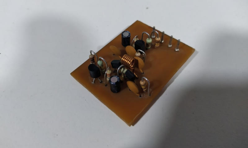
Anyone that has ever tried designing a VCO in the VHF/UHF range using discrete components know how much of a hassle that can be, and how many problems can arise from improperly picked components and/or bad PCB layout. Phase noise, frequency drift, signal distortion, impedance missmatch, oscillator not starting or starting after N seconds - problem I encountered with the following textbook version of a differential VCO made using two BJTs, etc.
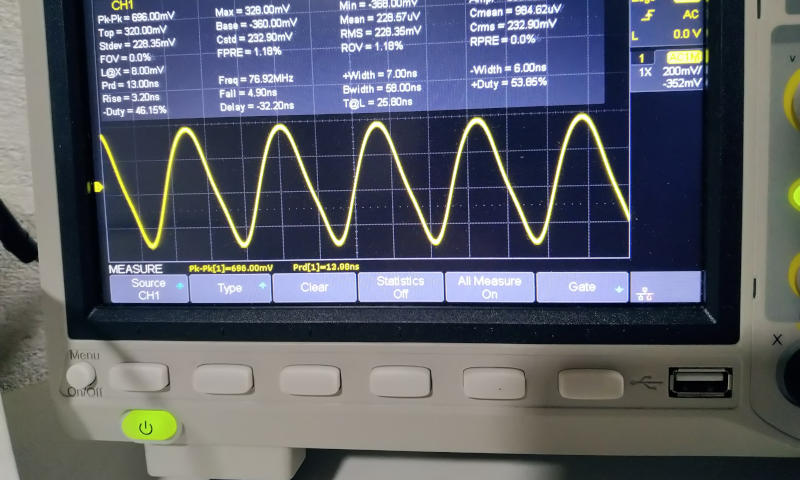
The specific issue of the oscillator not starting "seemingly" immediately occured due to the low gain of a differential amplifier. The amplitude "build-up" took 4 entire seconds and it was easily ammended by adding two bypass capacitors across the emitter resistors. It was made on a single-layer copper clad board and can generate frequencies in the VHF range between 30 and 80 MHz.
Revision 1 (Failure)
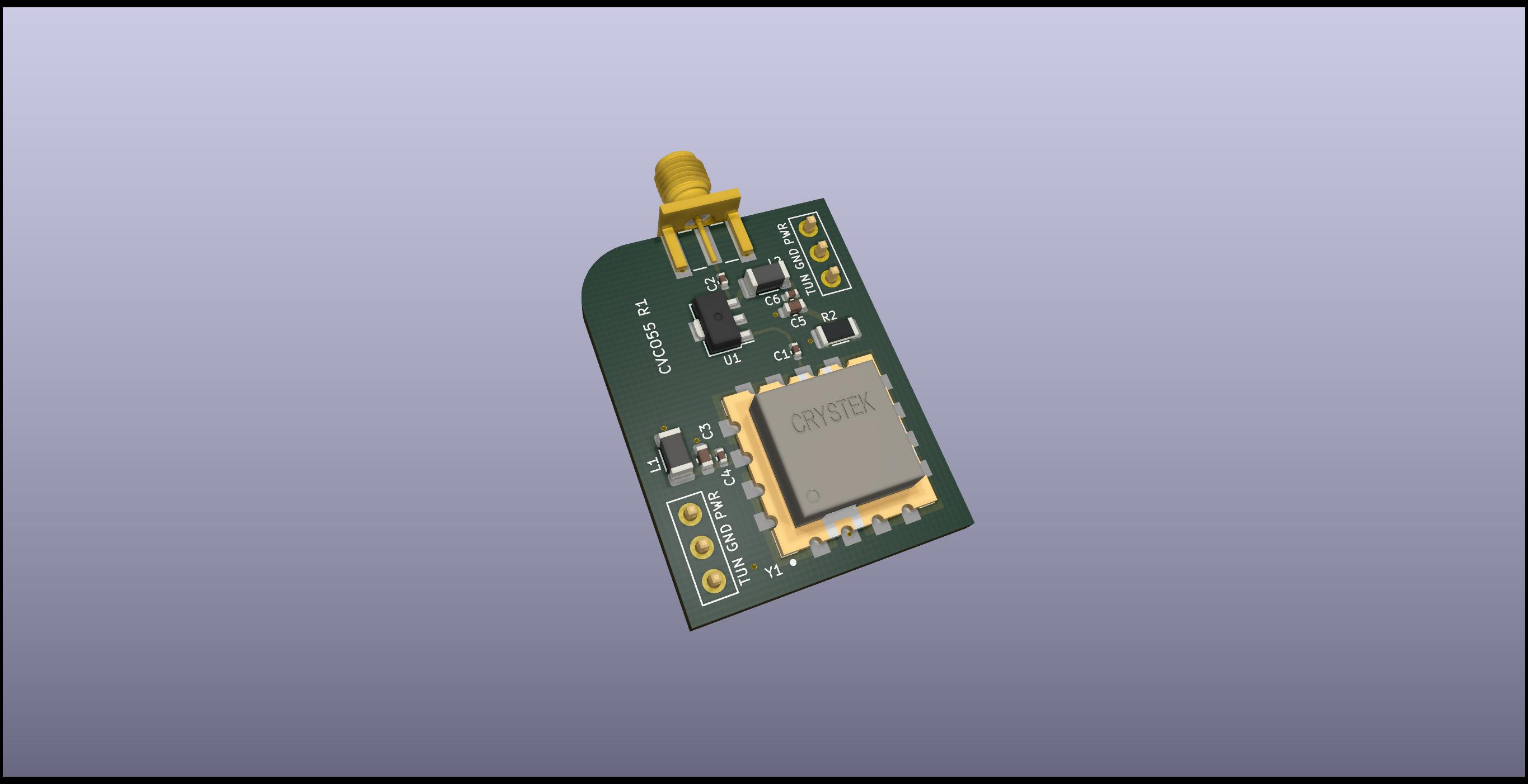
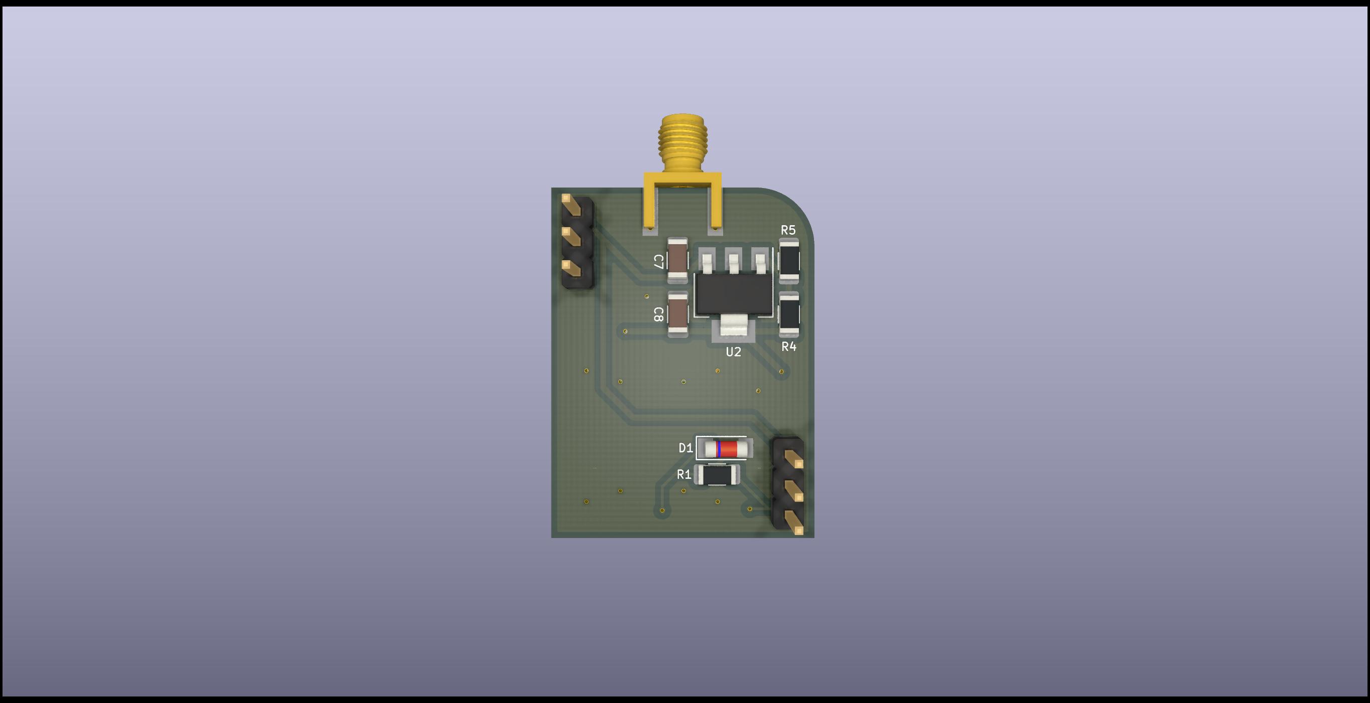
The first revision features an adjustable LDO as the voltage requirements vary from VCO to VCO, clamping and limiting circuit for the Tuning signal to keep it within VCO's specifications, and a broadband Gain Block from Qorvo (TQP369182) - boasting 20dB gain in the DC-6GHz range. Traces were kept as short as possible and matched to 50-ohm impedance to prevent power loss, reflections, etc. Unfortunately, as I was still "green" when designing this module, I made two mistakes that made it useless for anything other than low-power jammers.
I used a microstrip line to connect VCO's output to Gain Black with a 90-degree bend, without taking the bend into the account, and chosen the Gain Block poorly. The bend altered the desired impedance, and the components placed near the trace didn't help either. Chosen Gain Block's compression point was around 15dB, while the average output of a VCO from Crystek was around 10dB - which brought down the signal amplification from the boasted 20dB to the average 5dB and introduced a lot of unwanted distortions and harmonics.
In addition to that, the board is lacking stiching vias - but that is of little to no concern with all of the mentioned problems. Luckily, we live in the golden-age of prototyping, and the cost of a 4-layer board of this size (with controlled impedance) is only 2$ including Shipping - from China to Serbia at-least.
Revision 2 (Success)
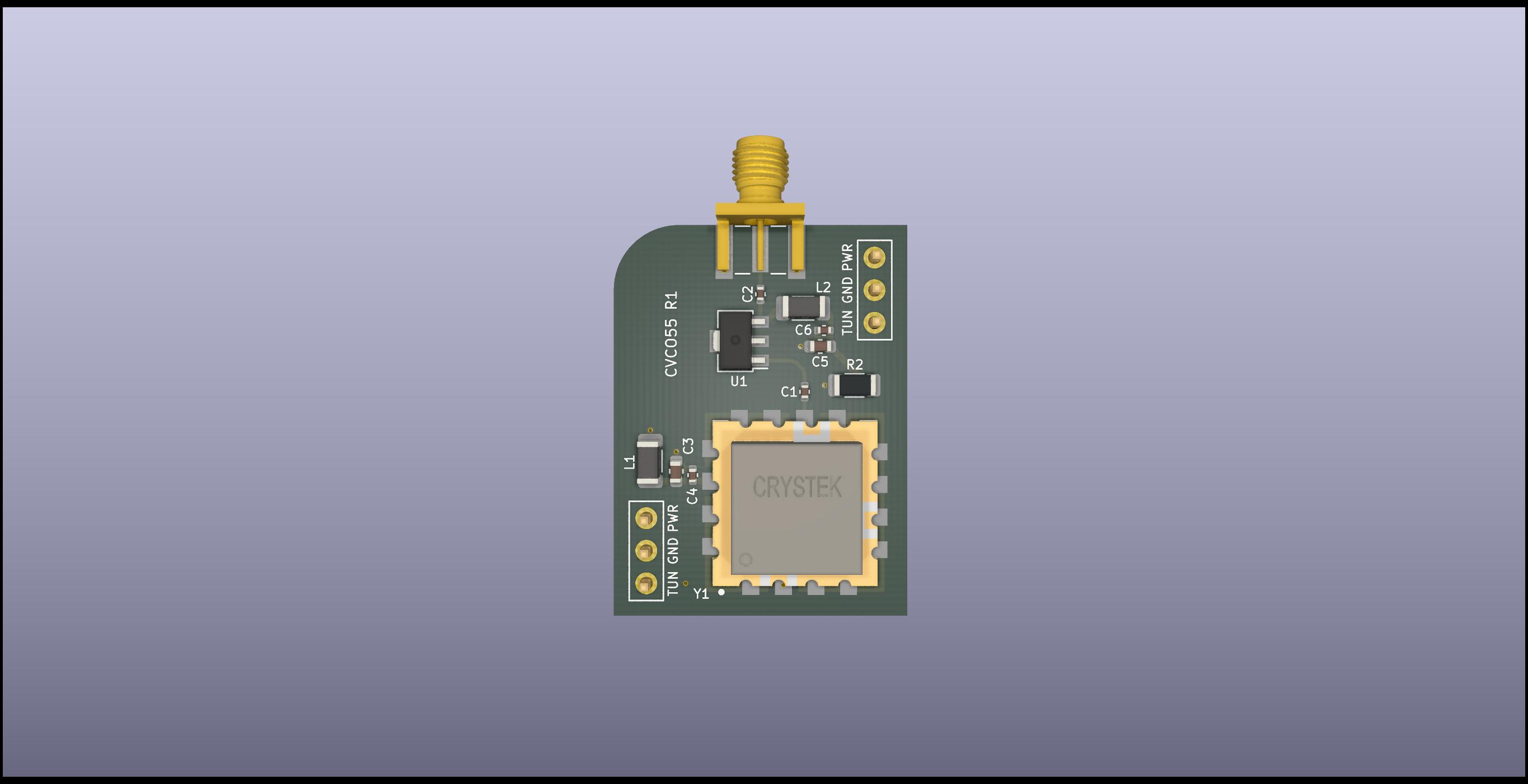
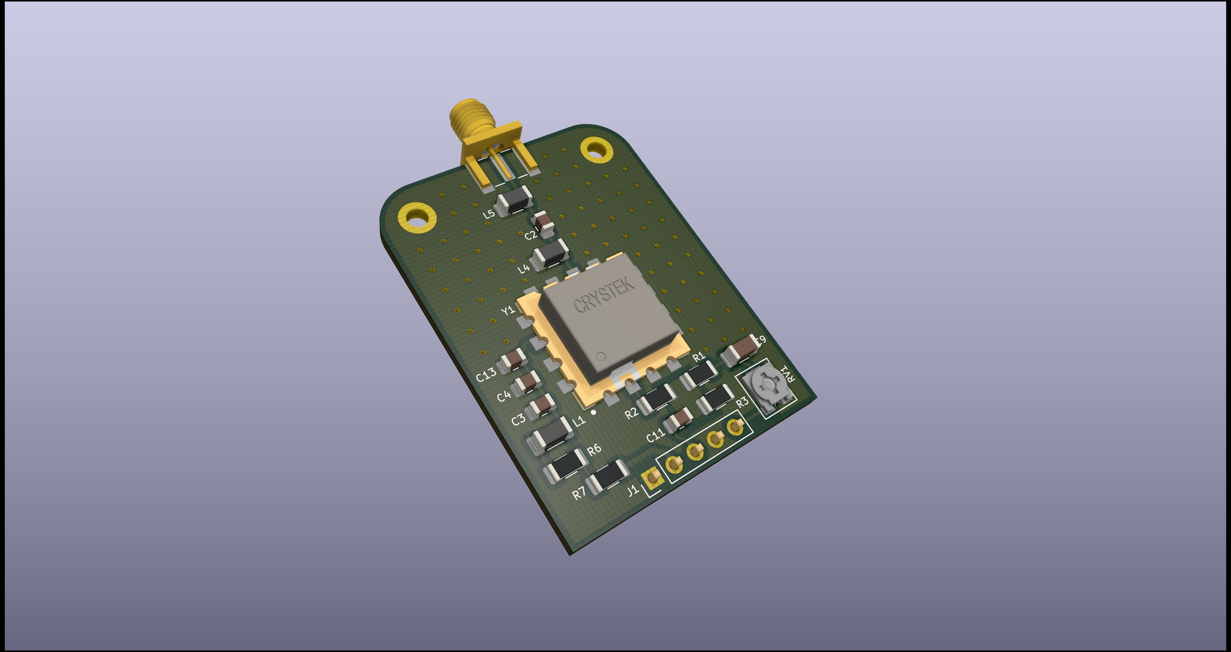
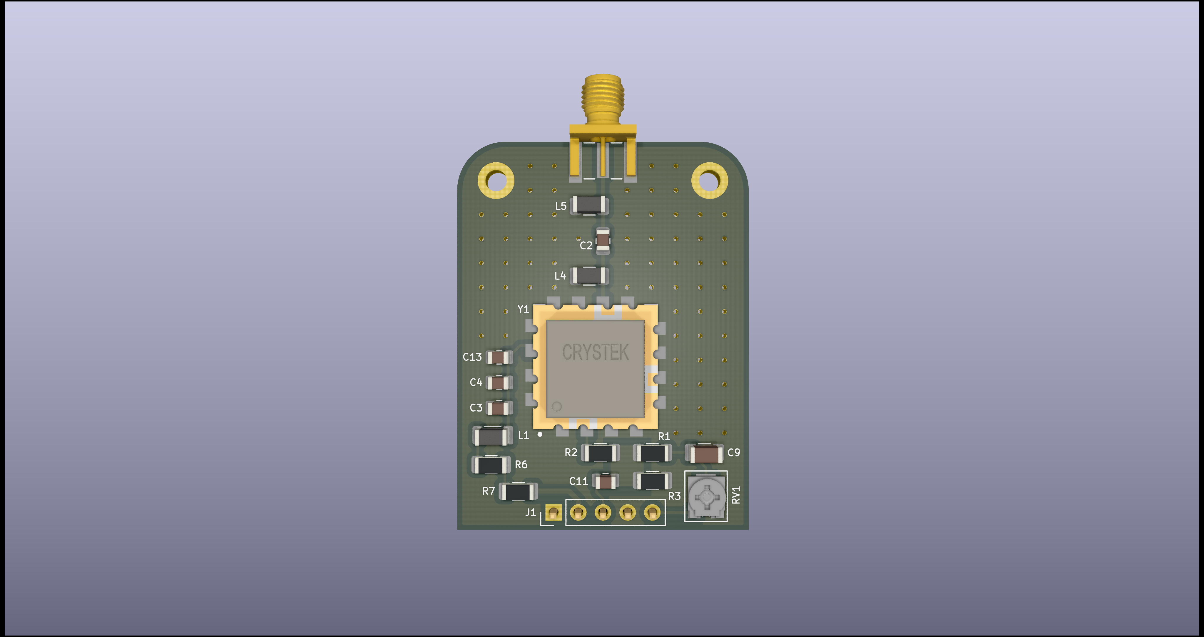
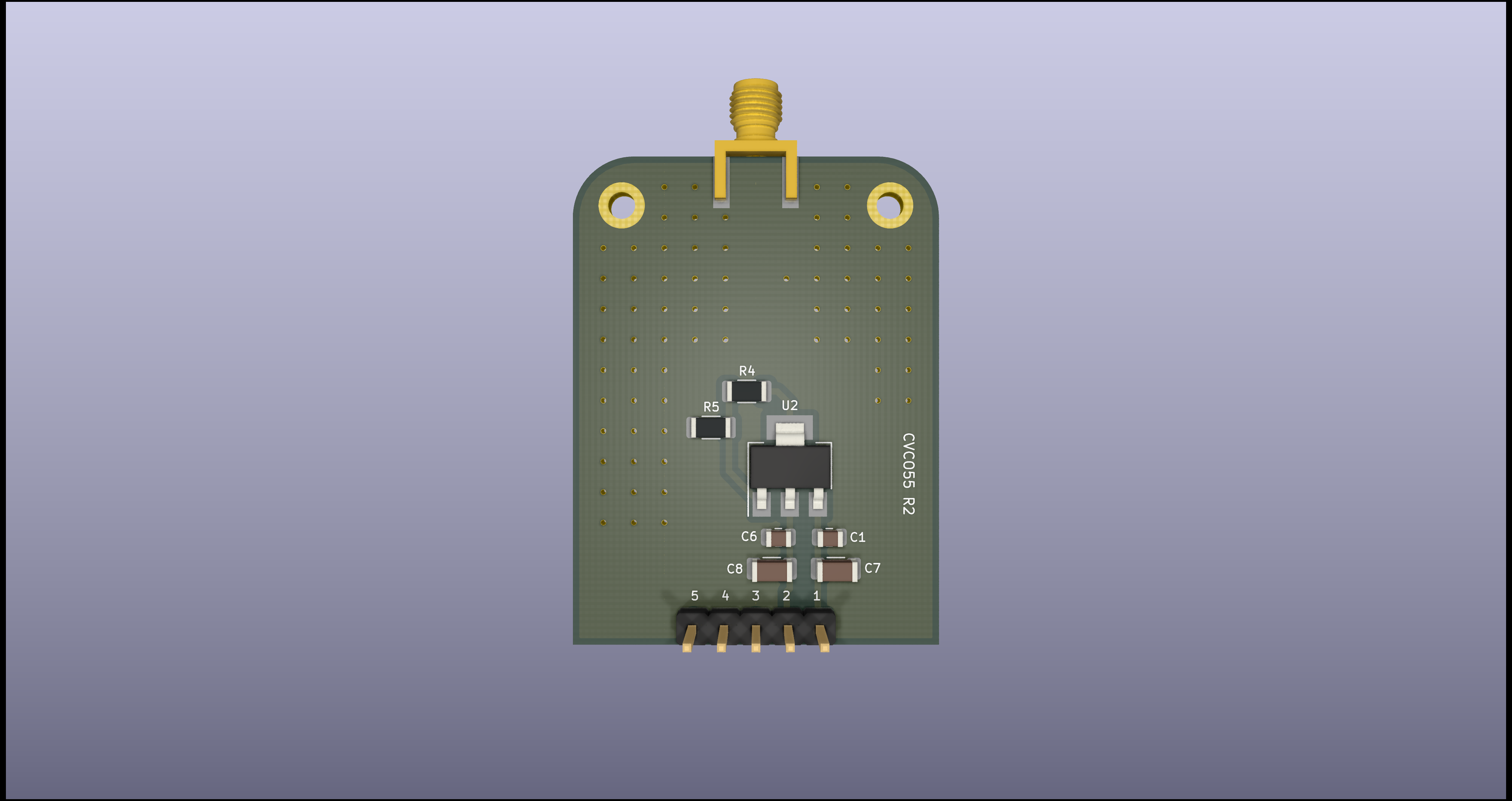
All of the issues from the previous version were addressed in this one. Power Output of cca. 10dB was sufficient for most of the use-cases I had in mind, so the problematic Gain Block was removed. Upon performing basic Circuit Analysis of the Tuning section, Clamping circuit was replaced with one that can provide a variable DC offset to the Tuning signal. Microstrip Transmission Lines were replaced with Coplanar Waveguide Transmission Lines, and a PI network was added just in case there was an Impedance mismatch. Last but not least, board was given that signature "RF" look through via stitching - not arbitrary one of-course. Assuming that the highest generated Frequency of a VCO could be 6GHz - using CVCO55BH-5840-6040, chosen distance between stitching vias was selected to be 2.5mm matching λ/20 for 6GHz wavelength.
